A DETAILED EXAMINATION OF THE “LERNAKIT” OSCILLOSCOPE
INTRODUCTION
This paper has been prepared with three basic aims in mind:
firstly, to recapitulate the material covered elsewhere in the
course as to what we want the Oscilloscope to do: secondly, to
deduce from this discussion the basic types of circuits needed
to satisfy our demands: and thirdly, to examine, in some detail,
the component parts of these 'circuit blocks’ so that you will
see the purpose of every resistor and capacitor. It is not
expected that you will fully understand all the points made on
first reading and some matters may remain obscure to you until
such time as your other reading and experimental work has
broadened your knowledge of electronics. However, you should
be able to follow this paper as far as the detailed examination
of Power Supplies.
In keeping with the basic policy of the “Lernakit" course,
this paper will not discuss any or the mathematics of the
Oscilloscope circuit - interested students should refer to the
many excellent texts available on valve theory - but will keep
Strictly to practical matters. Further, some typical faults
which can occur on the Oscilloscope are appended so that you may
attempt diagnosis as a means of testing your understanding of the
circuit operation.
Before proceeding further, some general points of
nomenclature:-
(1) Where electrodes of a valve are referred to, the
relevant base holder pin number will be inserted in
parentheses - e.g. V2 anode (7)
(2) In general, component values will not be used, only
the component designator (C19, R11 etc.) These may
appear in the text and on the diagrams, and do, of
course, relate directly to the "Oscilloscope Complete
Circuit Diagram", a copy of which is attached for
reference.
Finally, a word of caution - this paper is designed to assist
You in fully understanding one particular Oscilloscope, and,
therefore, you should not generalise from the details given
here when dealing with other Oscilloscope circuits.
The Basic Problem
When assembly of the Oscilloscope is complete, to what
uses shall we put it? The broad answer is that we will use the
instrument to examine the alternating voltage waveforms that
are present in the many electronic circuits which we shall
encounter.
We can go further and state that some of these
waveforms will have a high frequency, whilst others will have
a low frequency: some of these waveforms will already be large
whilst others will be so small that we will have to boost them
to a suitable level for display on the O.R.T. Finally, if the
Oscilloscope is to be of any use in servicing and design work, it
must not introduce significant distortion to the applied signal
or else the results of tests will be of little value.
"From this, the basic requirements to be met in the design
of the Oscilloscope are:—
(1) The ability to display clearly signals of high and
low frequency,
(2) The ability to reduce (attenuate) large signals and
boost (amplify) smell signals so that either type may
be clearly seen on the C.R.T.,
(3) The ability to present the applied signal in an
undistorted manner on the C.R.T., and, of course,
(4) The Instrument must function when connected to the
normal domestic electricity supply.
Before proceeding with a detailed examination of these
requirements, resulting in the establishment of a design based
on ‘circuit blocks’, the results of voltage superimposition will
be discussed.
Voltage Superimposition
By mathematical convention the horizontal axis of a graph
is labelled 'x' and the vertical axis 'y' (as the purpose of V1
is to disturb the vertical position of the timebase, it is
called the 1-Amplifier valve) 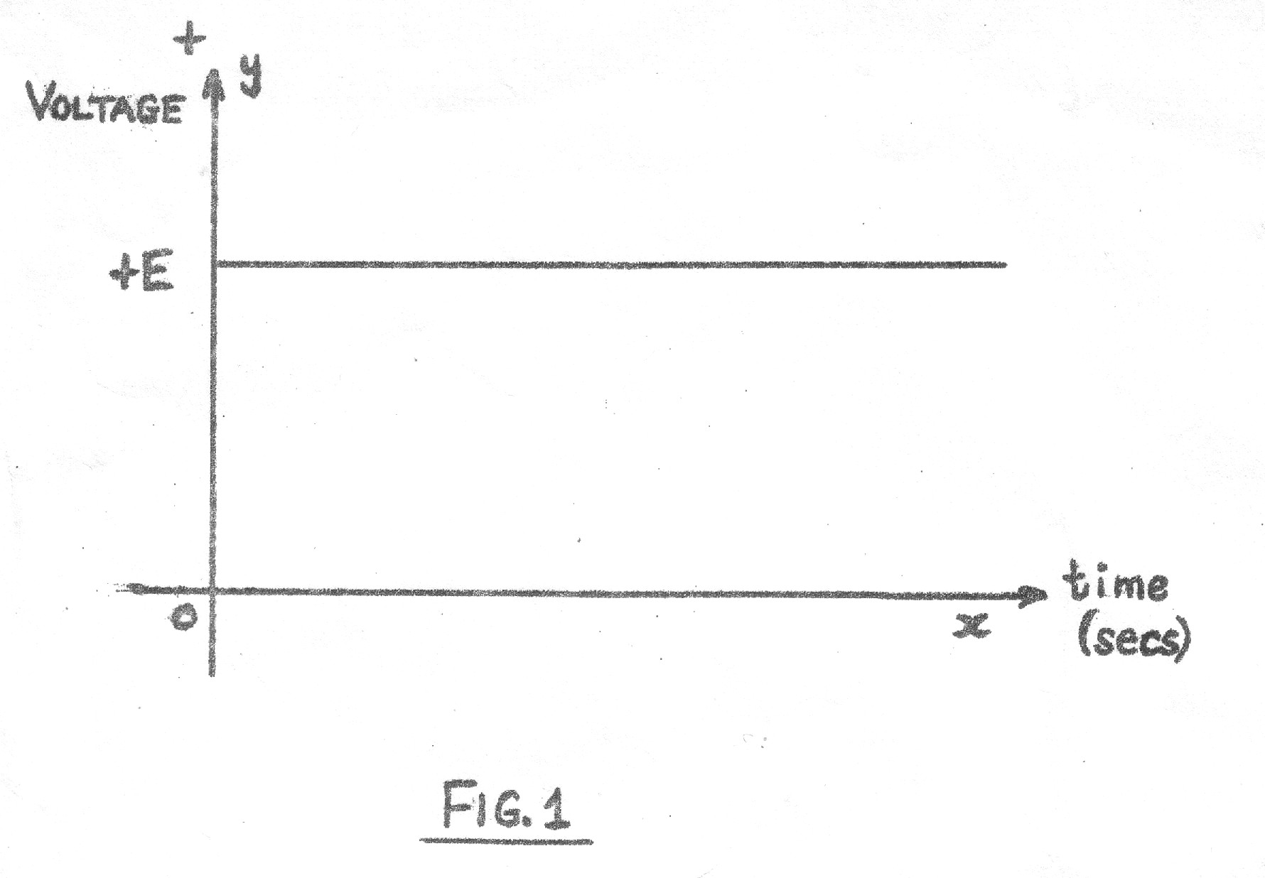
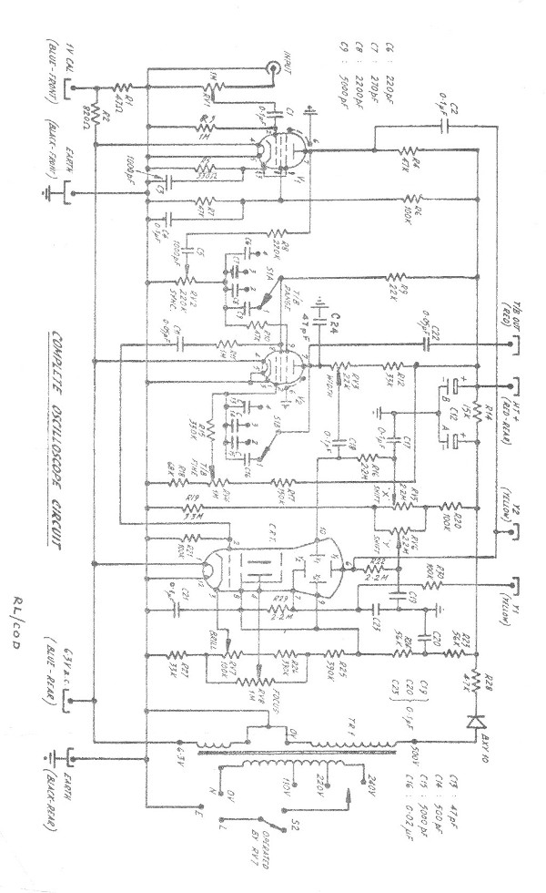
In fig. 1, the horizontal (x) axis represents time (in
seconds) and the vertical (y) axis represents voltage. The
graph shows a steady, positive voltage as would be produced
by a battery - you will notice that the value of this voltage
is constant with respect to time. i.e. +E volts.
On the other hand, Fig. 2. shows the familiar sine wave
alternating voltage, and here, the time at which we "look" at
the voltage does affect the value obtained. For example, at
time t1, the voltage is zero, at time t2 negative, and
at A and B the voltage reaches its maximum of +/- e volts.
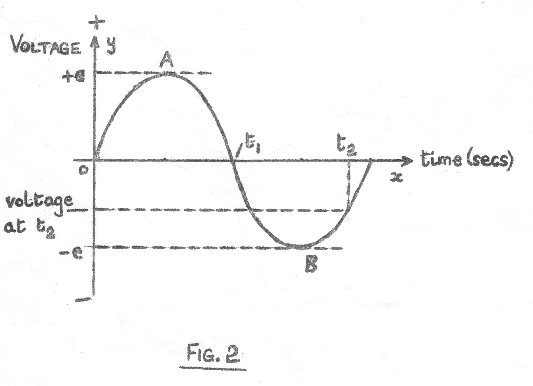
Suppose now that, in some way, we superimpose a small
alternating voltage on top of a fixed, steady voltage. the
two component parts are shown in Fig. 3 on the sane graph. to
find the effect of the superimposition, we take a point in time
and measure the value of each of the two voltages in Pig. 3.
We then add these two values together and plot the new voltage
obtained. Thus, at time t1, the fixed voltage has a value of
+E volts and the alternating voltage has a value of +e volts -
the sun or these two values is +(E+e) volts and this is the
value which we shall plot our "result" graph at time t1.
The "result" graph is shown in Fig, 4 and it has been derived
by adding the instantaneous (Fig. 3) voltages for every
moment in time.
Notice particularly in Fig.4 that although the
graph shows an alternating voltage, the instantaneous value of
voltage is never negative - only more-and-less positive.
Thus, by superimposing a small alternating voltage onto
a large steady voltage, we retain the alternations without ever
creating a negative voltage value. This concept appears quite
often in electronics - for example, to obtain distortion - free
amplification, it is necessary to ensure that the control grid
of a valve is always negative with respect to the cathode. This
is done by applying a fixed, steady negative voltage to the grid
and then arranging that the signal to be amplified has a maximum
value somewhat less than the fixed voltage. The effect of this
superimposition is to keep the grid negative with respect to the
cathode at all times.
We now return to discuss the four design considerations
in more detail.
(1) The ability to clearly display high and low frequency
signals.
The electron beam in the C.R.T. is, because it consists
of a stream of negatively—charged electrons, attracted by a
plate carrying a positive charge. Therefore, to each
X-plate we apply the some positive voltage and, since each
plate attracts the electron been with the some "pull", the
spot of the C.R.T. face will remain central. By applying
like voltages to the Y-plates, we stop the spot drifting up
and down over the tube face. with only these voltages applied
to the cathode ray plates, the spot will remain in the
centre of the C.R.T. face. If now, we apply an alternating
voltage like that in Fig. 5(a), it will be superimposed onto the
steady, fixed voltage of the Y2-plate, previously described.
Therefore, the Y2 plate voltage will vary in a "more-or-less"
positive manner, exactly as in Fig. 4. However, since the
voltage on the Y1-plate remains constant, the spot will now
move since we have disturbed the balance of electrical forces
across the Y-plates. So, when the voltage on Y2 is made more
positive by the addition of the fixed voltage and the
alternating voltage (e.g. t1 in Fig. 4), the electron bean
will be pulled down.
(Students who have performed Experiments
1 & 2 will be aware that, as you look at the face of the tube
in the completed Oscilloscope, the Y1-plate is at the top of
the tube and the Y2 plate is at the bottom. The X—plates are
laid out as shown in the theoretical circuit, i.e. X1-plate
to your left and X2-plate to your right).
Conversely, when the voltage on the Y2-plate is made less
positive (e.g. t3 in Fig. 4), the Y1-plate voltage will be
greater than this and it will attract the electron beam up
towards the Y1-plate. Because the spot travels so quickly and
due to the "persistence" (or "after-glow") of the coating on

the inside of the tube face, the trace on the C.R.T. would be a
straight, vertical line as shown in Fig. 5(b). Since the
wave-form in Fig. 5(c) would produce exactly the same picture
on the C.R.T. face, it is obviously necessary to "spread" the
picture out across the tube so that we can differentiate between
the types of waveform likely to be applied to the Y-plates.
This is the purpose of the TIMEBASE CIRCIn fig. 1, the horizontal (x) axis represents time (in
seconds) and the vertical (y) axis represents voltage. The
graph shows a steady, positive voltage as would be produced
by a battery - you will notice that the value of this voltage
is constant with respect to time. i.e. +E volts.
On the other hand, Fig. 2. shows the familiar sine wave
alternating voltage, and here, the time at which we "look" at
the voltage does affect the value obtained. For example, at
time t1, the voltage is zero, at time t2 negative, and
at A and B the voltage reaches its maximum of +/- e volts.
Suppose now that, in some way, we superimpose a small
alternating voltage on top of a fixed, steady voltage. the
two component parts are shown in Fig. 3 on the sane graph. to
find the effect of the superimposition, we take a point in time
and measure the value of each of the two voltages in Pig. 3.
We then add these two values together and plot the new voltage
obtained. Thus, at time t1, the fixed voltage has a value of
+E volts and the alternating voltage has a value of +e volts -
the sun or these two values is +(E+e) volts and this is the
value which we shall plot our "result" graph at time t1.
The "result" graph is shown in Fig, 4 and it has been derived
by adding the instantaneous (Fig. 3) voltages for every
moment in time.
Notice particularly in Fig.4 that although the
graph shows an alternating voltage, the instantaneous value of
voltage is never negative - only more-and-less positive.
Thus, by superimposing a small alternating voltage onto
a large steady voltage, we retain the alternations without ever
creating a negative voltage value. This concept appears quite
often in electronics - for example, to obtain distortion - free
amplification, it is necessary to ensure that the control grid
of a valve is always negative with respect to the cathode. This
is done by applying a fixed, steady negative voltage to the grid
and then arranging that the signal to be amplified has a maximum
value somewhat less than the fixed voltage. The effect of this
superimposition is to keep the grid negative with respect to the
cathode at all times.
We now return to discuss the four design considerations
in more detail.
(1) The ability to clearly display high and low frequency
signals.
The electron beam in the C.R.T. is, because it consists
of a stream of negatively—charged electrons, attracted by a
plate carrying a positive charge. Therefore, to each
X-plate we apply the some positive voltage and, since each
plate attracts the electron been with the some "pull", the
spot of the C.R.T. face will remain central. By applying
like voltages to the Y-plates, we stop the spot drifting up
and down over the tube face. with only these voltages applied
to the cathode ray plates, the spot will remain in the
centre of the C.R.T. face. If now, we apply an alternating
voltage like that in Fig. 5(a), it will be superimposed onto the
steady, fixed voltage of the Y2-plate, previously described.
Therefore, the Y2 plate voltage will vary in a "more-or-less"
positive manner, exactly as in Fig. 4. However, since the
voltage on the Y1-plate remains constant, the spot will now
move since we have disturbed the balance of electrical forces
across the Y-plates. So, when the voltage on Y2 is made more
positive by the addition of the fixed voltage and the
alternating voltage (e.g. t1 in Fig. 4), the electron bean
will be pulled down.
(Students who have performed Experiments
1 & 2 will be aware that, as you look at the face of the tube
in the completed Oscilloscope, the Y1-plate is at the top of
the tube and the Y2 plate is at the bottom. The X—plates are
laid out as shown in the theoretical circuit, i.e. X1-plate
to your left and X2-plate to your right).
Conversely, when the voltage on the Y2-plate is made less
positive (e.g. t3 in Fig. 4), the Y1-plate voltage will be
greater than this and it will attract the electron beam up
towards the Y1-plate. Because the spot travels so quickly and
due to the "persistence" (or "after-glow") of the coating on
the inside of the tube face, the trace on the C.R.T. would be a
straight, vertical line as shown in Fig. 5(b). Since the
wave-form in Fig. 5(c) would produce exactly the same picture
on the C.R.T. face, it is obviously necessary to "spread" the
picture out across the tube so that we can differentiate between
the types of waveform likely to be applied to the Y-plates.
This is the purpose of the TIMEBASE CIRCUIT and we shall consider
this now, assuming for the moment that the Y-plate alternating
voltage has been removed leaving only the fixed X and Y-plate
voltage for spot centering purposes.
Suppose that we apply the relatively~small alternating
voltage shown in Fig.6 to the X1-plate. At time t1, the
combined voltage (fixed + alternating) on the X1-plate is more
positive than the fixed voltage on the X2-plate - the spot will
be pulled to the left. Immediately after t1, the X1-plate
voltage begins to fall and, as it does so, the "pull" on the
spot by the X-plate falls causing the X2-plate to steadily
attract the electron been so that the spot moves steadily to the
right, until, at time t2, the pot is well over to the right-
hand side of the C.R.T. face (X1-plate voltage is now less than
the fixed voltage on X2). In the time interval between t2 and
t3, the X1-plate voltage rises rapidly back to its original
value, thus pulling the spot quickly back to the left-hand side
of the tube and this cycle continues with the spot moving
relatively slowly from left to right (e.g. t1 to t2) and
relatively quickly from right to left (e.g. t2 to t3). Because
the spot moves beck so quickly, we say that is "flies back".
Notice particularly that the voltage on the X1-plate falls
steadily between t1 and t2 so that the spot moves from left
to right at a steady,speed. Fig.7 shows the positions of
the spot at the beginning of its traverse, at the end and at
three points in between such that each point is, time-wise
equidistant from its neighbour. We shall now have this voltage
on the X1-plate and reconnect the Y-plate sine wave signal to
see the combined effect.
Fig. 8(a) shows three cycles of a sine wave labelled
Z, Y, and Z. when you are servicing equipment with the
Oscilloscope, you will he looking at signals having
frequencies of anything from 20 cps upwards. Thus it
there are 20 cycles in one second, the time taken by one
cycle is 1/20th seconds. To avoid such fractions in
this discussion, we shall say that the time taken for one
cycle in Fig. 8(a) is 4T seconds and bear in mind that
4T is a fraction of a second.
Therefore, in Fig.8(a),after T seconds the value or the sine wave signal is its positive maximum; after 2T seconds it is zero; after 3T seconds its maximum negative value and, after 4T seconds it is zero again.
Fig. 8(b) shows the alternating voltage which is
being applied to the X1-plate and you can see that it too
takes 4T seconds to go through one complete "sawtooth"
cycle. Since it is not possible to raise the sawtooth
voltage from its maximum negative value to its maximum
positive value (i.e. from C1 to D1) in zero time, we
shall use 't' here to mean short period of time taken
by the sawtooth voltage to raise. As 't' is the time taken
by the spot on the C.R.T. face to return to the left-hand
edge from the right edge, "t' is the "flyback time", and
D1 corresponds to (4T + t) seconds from the start. Let us
examine now what we shall see on the tube face and, to
simplify the work; we will start by considering the point
2T seconds after the start.
The alternating components applied to the Y2-plate is
thus zero so that the electron beam will, under the action
of the Y-plates alone, be on the horizontal axis of the tube
face. However, at the same time, the alternating voltage
on the X1-plate is slightly above zero so this will
position the spot slightly to the left or the centre of
the tube face. The combined effect of these two voltages
will be to position the spot at P in Fig. 8(c) (0 is the centre of the C.R.T. face).
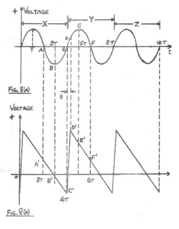
Now consider the case T seconds later (3T seconds after the start). The sine
wave voltage applied to the Y2-plate will be at B in Fig.8(a) and this will position the spot above the horizontal axis of the C.R.T. face (Voltage on Y2 less than that on Y1 so Y1-plate pulls the spot up). At this same time the
voltage applied to the X1-plate will have fallen to the value at B1 and, since this negative, the X1-plate voltage will be less than the X2 plate voltage thus
allowing the X2-plate to pull the spot to the right of centre, The combined effect of these two voltages is to position the spot at Q(Fig. 8 (c).
4T seconds after the start, the voltage applied to the Y2-plate is zero (see Fig. 8 (a) and that applied to the Xl-plate is its maximum negative value so that the spot will be as far to the right as possible and on the
Horizontal axis i.e. at R in Fig. 8 (c). With the rapid voltage rise that takes place on the X1—plate between time 4T seconds and time (4T + t) seconds, the spot flies back to the left-hand edge of the C.R.T. face. During this same time interval the sine wave voltage rises from the C to D Fig. 8 (a) so that (4T + t) seconds after the start, the spot will be at S. 5T seconds after the start, the
Y2-plate voltage will have risen to its value at E, plus the fixed voltage: the voltage on the X1-plate will have fallen slightly to its value at E1, plus the fixed voltage and the spot will be at U in Fig. 8 (c). 6T seconds after the start, the voltage on the Y1-plate will equal that on the Y2-plate and the X1 plate voltage will have fallen to the same value as it had 4T seconds earlier (i.e. at A1).
Therefore, the spot will be back at P and if now you continue to deduce the positions of the spot for the rest of sine wave cycle Y, cycle Z etc., you will exactly "overlay" the points already plotted in fig. 8 (c). Further,by
considering all the intermediate points (between A and F for example),you will plot a sine wave of fig 8(c).
Thus, by applying the voltage in Fig. 8 (a) (on top of the fixed voltage) to the Y2-plate and, at the same time, applying the voltage in Fig. 8 (b) (on top of the fixed voltage) to the X1-plate, a "picture" of the Y2-plate, alternating signal appears on the C.R.T. face due to the persistence of the screen coating.
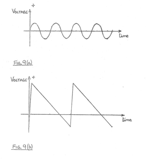
A very valuable exercise is for you to use the above method to deduce the picture which will appear on the C.R.T. face if we apply the voltage shown in Fig. 9 (a) to the Y2-plate and the voltage shown in Fig. 9 (b) to the X1-plate. The answer is shown in Fig 9 (c).
Notice here that because the sawtooth voltage goes through one cycle in the some time as the sine wave voltage goes through two circles, two cycles of the sine wave voltage will _ appear on the C.R.T. face. Therefore, to enable us to
clearly display voltage waveforms having high and low frequencies, we must have not only the circuitry to generate the sawtooth X-plate voltage but also the circuitry to vary the time taken in one cycle of this sawtooth
voltage. Because of its close relation with time, the sawtooth-generating circuit is called the Timebase Generator. Also, if one cycle of an alternating voltage takes one fiftieth of a second, then we shall get 50 such cycles in
one second; i.e. in general terns, if 'f' is the frequency in cycles/second and 't' is the time for one cycle (in seconds), then f = 1/t. So, we can conclude that the Oscilloscope must have a Variable Frequency Timebase Generator
circuit to enable us to clearly display alternating voltages of both high and low frequency.
Three Small Points
(1) Careful inspection of Pigs. 8(c) and 9 (c) shows that the entire picture is slightly left of centre. We correct this by slightly reducing the steady, fixed voltage applied to the X1-plate as this effectively shifts the entire trace to the right without distorting the picture in-any way.
(2) Also, it is apparent from Figs. 8 (c) and 9 (c) that a part of the picture display was not present in the sine wave signal applied to the Y2-plates.
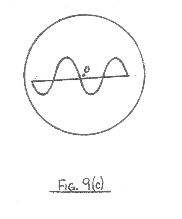
This unwanted pert is the flyback line (RS in Fig. 8(c) and we remove this by arranging an output from the timebase generator circuit which completely cuts-off the electron beam whilst the sawtooth voltage is rising rapidly.
This output is called the Flyback suppression (or Retrace Blanking) pulse - note that it must be generated by the Timebase Circuit since the flyback suppression pulse must be synchronised to the rise in sawtooth voltage or else we might blank out the wrong part if the trace.
(3) You may have wondered why, in the discussion relating to Figs. 8 (a), (b), and (c) above, we began by considering the point 2T seconds after the start. The reason for this is as follows.
If you-will return to Figs. 8 (a) and 8 (b) and consider only the first cycle of the timebase voltage and cycle 'X' of the sine wave, by deduction in the usual way,
you will obtain a picture exactly like Fig. 8 (c). Careful inspection of cycle X (fig. 8 (a) and Fig. 8 (c) shows that we have in fact obtained a picture on the C.R.T. face which is a "mirror image" of the signal applied to the Y2—plate.
(This is because the Y2-plate is at the bottom of the tube as you lock at it). This was done deliberately because the Y2-plate signal is normally derived from the Y-amplifier and the output of this valve is a "mirror image!
of its input.
Thus, if we apply cycle X of Fig. 8 (a) to the Y-input
socket, the output of the Y-amplifier is a mirror image of
this signal. This is applied to the Y2-plate producing
another mirror image on the C.R.T. face. Obviously, the
two mirror image effects cancel each other out so that the
C.R.T. picture is a true replica or the Y-input signal.
X and Y Shift.
You will recall that to centre the picture on the screen it is necessary to apply fixed, steady voltages to the X and Y-plates such that the fixed voltage on Y1 is
equal to the fixed voltage on Y2 and the fixed voltage on X1 is slightly less than the fixed voltage on X2.
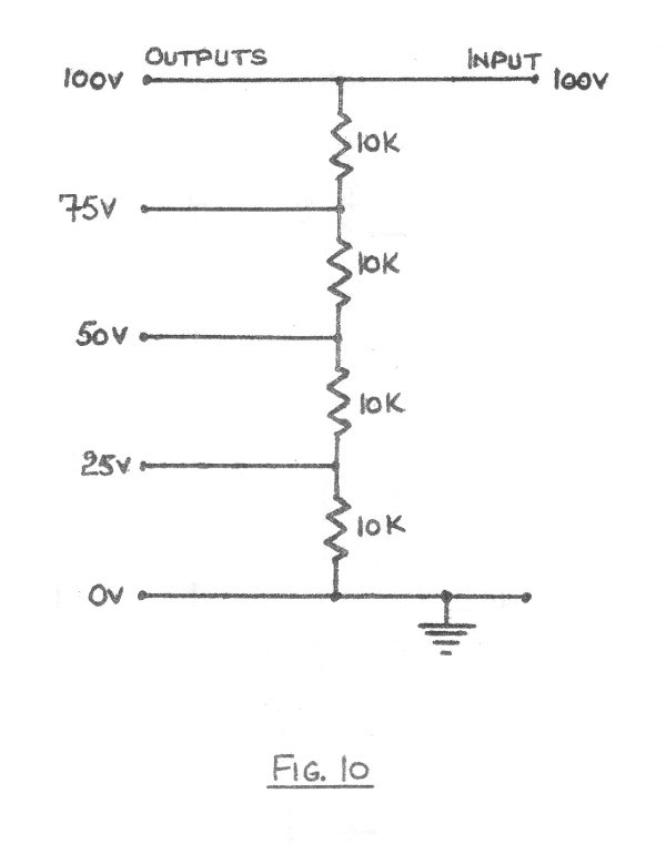
Now, fixed voltages are usually derived from a chain of resistors in series. The voltages at the various intersections then get less as you go down the chain
towards the earthy-end (of Fig.10) and this is called a POTENTIAL DIVIDER NETWORK as it divides the applied voltage (or potential) viz. 100V in this case. However, you know that all resistors have a + or - tolerance on
them and, therefore, it is very difficult to get a whole batch of resistors all or exactly the same value (this would be necessary if we want to pick exactly the same‘ voltages off of two networks). So, to balance out the differences between individual Oscilloscope networks, we must include controls to enable exactly the right, steady voltages to be applied to the X and-Y-plates to centre
the picture. It we arrange that the amount by which we can adjust these voltages is relatively large, then we can also use these controls to shift the entire picture either up and down (Y-shift) or from side to side (X-shift).
Focus and Brilliance
The Brilliance of the spot is varied by applying a
positive voltage to the cathode of the C.R.T. In order
that we can adjust the brilliance of the trace, a control
is provided. When the control is set, a fixed, steady
voltage is applied to the C.R.T. cathode (3), controlling
the number of electrons leaving the cathode and thereby
the brilliance of the spot. Because electrons are
negatively charged, the more positive the cathode voltage,
the dimmer the C.R.T. trace.
The Focus of the beam is varied by applying a controlled,
fixed voltage to the C.R.T. focussing anode (4).
The control allows the electron beam to be focussed after
its brilliance has been adjusted.
To force the electron beam down the tube from cathode
to screen face, we also have to apply a positive, fixed
voltages to the accelerating anode (8) of the C.R.T.
For the moment, only note these facts and remember
that the brilliance, focus, and beam acceleration are
controlled by steady positive voltages - the method
for getting the necessary voltages and for varying them to
achieve a good picture will be discussed later.
The C.R.T. Control Grid (2)
In view of its proximity to the cathode in the C.R.T.,
a relatively small voltage change on the control grid (2)
considerably affects the number of electrons leaving the
electron gun assembly. If we apply a small, negative
voltage to the control grid, virtually all the electrons
leaving the cathode will be repelled by the grid and thus
the spot on the C.R.T. will disappear. Therefore, if we
connect the Flyback Suppression pulses to the control grid,
we will blank off the unwanted part of the trace (RS in
Fig, 8 (c).
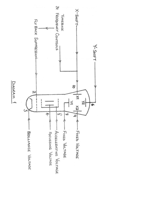
We have now discussed enough material for the first
parts of our Oscilloscope block diagram to be constructed.
This is shown in Diagram 1 and you should study it in
conjunction with all the previous notes until you feel sure
that you understand its derivation. With the lengthiest
piece of discussion over, we can now relax a little and
discuss the remaining requirements previously listed.
The ability to clearly display large and small signals
It will be obvious that some signals will be so small
that they will hardly disturb the timebase (vertically) at
all whereas other signals will be so large that, when
displayed on the G.R.T., they will "drive" the tube so hard
that most of the trace will be off the screen. Therefore,
we must include the necessary circuitry to amplify small
signals and attenuate large signals so that, irrespective
of signal input size, we can control the displayed waveform
to our liking.
The technique which we shall use is to attenuate all
signals and than amplify them.
This is done because the occasions when a signal that will exactly produce a good picture are relatively few. So we attenuate everything by an amount between 0% and 100% and thereby select a voltage which we can amplify to obtain the best C.R.T. picture.
The attenuator on the Oscilloscope circuit consists
of a potentiometer (RV1). As we have already referred to
the focus, brilliance, X and Y-shift-controls, this will
be a suitable point to revise the operation of a
potentiometer.
Firstly, consider four resistors in series as in
Fig. l0. One end or the network is connected to earth and
the other end to a voltage source (either AC or DC). 0hm's
Law enables us to calculate the voltage which appear at the
junctions of the resistors and this is done in Fig. l0 for
a supply of 100V. Now, the resistors commonly used are a
form of carbon so if we now imagine that we "weld" all four
resistors together to make one long piece of carbon, we
still have our total resistance of 40K-Ohms. if you now
imagine that we scrape the paint etc., from the outside of
the carbon rod so formed, we could now touch a contact, not
just to the junction of the four original resistors, but
to any point. This would enable us to pick of any voltage
from 100V down to 0V.
The action of the Y-gain control and the other
potentiometers mentioned, is to enable us to apply one voltage
at one end, a different voltage at the other end, and to
pick off any intermediate voltage by simply turning a knob.
In the case or the Y-gain control, one end of the
potentiometer is connected to earth and we can pick off any
voltage between that applied to the other end of the carbon
track and zero. Thus, the control attenuates the applied
signal by an amount somewhere between 0% and 100% and,
since this attenuation is continuously variable, we can
"select" a suitably sized signal for amplification by V1.
We shall conclude this section by discussing the
remaining two requirements-
The ability to present the applied signal in an
undistorted manner is a point for the designer rather
than the student. Suffice it to say that every effort
has been made to optimise this factor.
Finally, we obviously must be able to run the
completed instrument from the domestic AC electricity
supply end, since the tube requires very high DC (EHT),
the valves high DC (HT) and the valve heaters low
voltage AC, we shall have to incorporate a suitable Power Supply Section. Thus, the complete block diagram
for the Oscilloscope takes the form shown in Diagram 2.
Please ensure that you fully understand this diagram before proceeding. We shall now discuss the circuit
blocks in more detail with reference to the specific
reason or each component. How much of the following
work will be clear to you will depend on where you are
in the course and how much extra knowledge you have
gained from general reading.
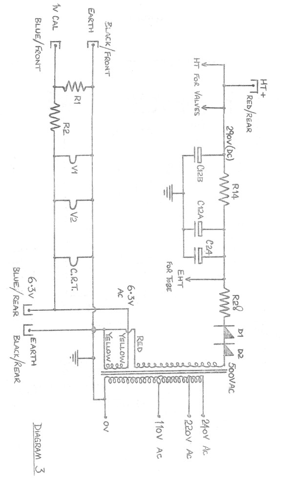
POWER SUPPLIES
The components forming the Power Supply section are
shown in Diagram 3. The circuit functions as follows:-
Alternating Current of either 110V, 220V, or 240V
is taken from the domestic electricity supply and applied
(via a 2 amp fuse for safety) to the primary of the mains
transformer. The voltage is stepped up by normal tarns-
former action to approximately 500V (AC) in the (red-wire)
secondary coil and down to 6.3V (AC) in the (yellow wire)
secondary coil. The latter supply is used to drive the
tube and valve heaters and also to provide the 1V 50 cps
calibration voltage from the potential divider network R1
and R2, the 1V peak-to-peak signal appearing at the junction
of the resistors. A 6.3V (AC) output is provided on the
rear panel for valve experiments.
The 500V AC is passed through the diode rectifier (s)
end then through R28. This resistor has virtually all the
current used in the EHT and HT circuits flowing through it
so, apart from the fact that it gets warm, it drops the
half-wave rectified AC down so that the "circuit" end of
R28 is about 410V (DC) and this is used to supply the
EHT for the tube. As virtually all the current used in
the V1 and V2 circuits flows through R14, a potential
difference exists across this resistor and this effectively
drops the EHT down to about 290V (DC) for the valve HT
line. In conjunction with R14, C12A and C12B form e pi-
section filter to remove most of the 50cps. hum which
would upset the valve and tube operation. C24 further
smooths out the DC on the EHT line. A lead is taken from
C12B to the red socket on the rear of the Oscilloscope to
provide the HT for the previously mentioned valve
experiments.
Thus, the circuitry shown in Diagram 3 provides the
necessary voltages to operate the Oscilloscope. These are:-
+ 410V (DC) for the C.R.T.
+ 290V (DC) for the valve circuits, and
6.3V (AC) for the valve and tube heaters.
N.B. Although the smoothing capacitors Cl2A and B, and
C24 reduce the AC component on the DC lines, they do not
completely eliminate it. Therefore, various 0.1 us
capacitors will appear in the circuit, their sole function
being to remove as much residual ripple as possible.
Derivation of the various voltages required by the C.R.T.
The voltages required by the C.R.T. i.e. fixed Y1-plate, fixed X2-plate, fixed accelerating anode, variable focus, variable brilliance; X-Shift and Y-shift are derived from the two potential divider networks shown in Diagram 4.
The networks function as described previously and the purpose of the components is as follows:-
(a) C11, C12, C20 and C23. - to remove unwanted 50cps
ripple and stabilise the tube voltages otherwise this ripple
would distort the picture on the C.R.T. since the voltages
on the Y1-plate and X-plate would not be steady.
(b) R20, Rv5 and RV6, R19 - these components form one
potential divider network to provide the X and Y-shift
voltages. R20 and R19 determine the limits of voltage
swing avai1able from the potentiometers RV5 and RV6, and these
two controls are fitted in parallel so that each slider picks
off the same range of voltages.
(c) R16 and R22 - to keep the voltage alternations coming
from the timebase generator (in the case of R16) and from the
Y-amplifier (in the case of R22) up at suitable levels, it is
necessary to fit two high-value resistors at R16 and R22.
If these resistors were omitted then the alternating waveforms
going to the X1-plate and to the Y-2 plate would be virtually‘
short away to earth via capacitors C17 and C19.
N.B. This is a convenient point to remind you that capacitors
resist any change in voltage. Also that AC "flows through"
a capacitor whereas DC is "blocked".
Therefore, if we connect a capacitor between the slider of
RV5 earth, the steady voltage coming off the slider will
be unaffected by the capacitor but any residual ripple will
be passed through the capacitor to earth. It also follows that
part of the timebase alternating voltage will pass to earth
through C17 but this is limited by the high-value resistor R16.
(d) C21 - in addition to helping to remove unwanted 50 cps
ripple from the Y1 X2-plates and the accelerating
anode, C21 earth's, AC wise, these electrodes. This is
necessary to ensure correct presentation of the time-base.
(e) R30 - direct access is provided to the Y-plates via
the two yellow sockets on the front panel. In normal use,
R30 does not impede the operation of this facility but, if
a test lead connected to the Y1 socket is inadvertently
shorted to earth or, if the user touches the metal of the
Y1 test lead and, at the same time, touches the chassis of
the Oscilloscope, capacitor C25 (which is charge up to about
+350V (DC) will discharge very rapidly.
The current flow,although brief, can give an unacceptable shock to the experimenter so this current flow is deliberately reduced
by resistor R3O. You will of course still get a shock if you
touch the chassis and the Y1-test lead at the same time but
the shock is not so great; R22 performs the same function for
the Y2-socket and C19 in addition to its previously described
purpose.
(f) R23., R24.,R25., R26.,RV7.,RV8 and R27 - these
resisters form the second C.R.T. voltage supply line and they
are connected in the form of a Potential Divider network.
R23 and R24 lower the voltage on the EHT line to a suitable
value for connection to the accelerating anode (8)., the Y1-
plate (7)., and the X2-p1ate (9). Two resistors are used
partly to give a suitable junction for the decoupling capacitor
C20. R25 and R27 limit the available voltage swing from RV8
(focus) to the desired range of values. R26 limits the
available voltage swing from RV7 (Brilliance) to the correct
maximum value and R27 sets the lower limit for RV7. (Because
the same lower limit is suitable for both RV7 and RV8., one
end of each control track is joined together. RV8 is in
parallel with R26 and RV7 because it needs a higher top limit
than the brilliance control - RV7). The slider
connection (2) on the Focus Control is routed to the C.R.T.
focussing anode (4) and the slider connection (2) on the
Brilliance Control is routed to the cathode of the C.R.T.
(3)
(g) R29 This resistor functions as R30 i.e. to protect
against excessive discharge currents in the event of in-
advertent short circuit from the Y1-socket to earth. In
this case, it is the discharge_current from C21 that is
being limited as, without R30 and R29., C21 could discharge
directly to the Y1-socket short circuit.
This concludes detailed examination of the tube EHT
voltage supplies, but, before proceeding with the Y-Amplifier
circuit, two points of general interest will be mentioned
as they arise from the discussion in the sections above.
(1) Component Numbering - by convention, component
numbers start at 1 and go up as you work across the circuit
from left to right. Thus, we see that the "highest" resistor
number on the Oscilloscope Complete Circuit Diagram is R30
and, knowing the convention and being asked to look at,
say R26.,we can immediately deduce that it will appear on
the right hand side of the Theoretical Circuit Diagram.
Although not so much of a problem on a small circuit such
as the Oscilloscope, you can imagine the usefulness of the
convention when trying to locate R69 in a colour television
receiver.
Sometimes, you will meet variations on the above method;
for example, in a stereo amplifier, all components having
an odd number may be in left-hand amplifier channel whilst
all components having an even number will be in the right
hand channel - but the basic rule of reading from left to
right still applies (R29 in the Oscilloscope is to the left
of R23-R27 because it was added as a modification).
(2) Voltage measurements - students who possess a test-
meter and who have measured some of the voltages in the
Oscilloscope may have wondered why a figure of 350V was quoted
in section (d) above for a voltage on C23. You will perhaps,
have measured a voltage of about 345V on pins 8 & 9 of the C.R.T.
base and a voltage of about 280V on pin 7. The immediate reaction
is to assume that sufficient current flows through R29 to cause
the voltage to drop across the resistor but closer inspection
will leave you wondering just where this circuit current flows
to. Diagram 4 shows that the only route this current flow could
take is through C23 to earth but; if this capacitor is functioning
normally, we know that DC does not flow through it.
The solution to this apparent anomaly lies in the method
used to measure the voltages and, because this problem can arise
in any circuit, we will justify the 350V potential on C23 before
continuing.
Fig. ll shows the C.R.T. Potential Divider Network (with
capacitors omitted because no DC flows through them) and, because
the tube itself does not draw any current from this part or the
circuit, the wires connecting R29., etc., to the tube are shown
as "dead ends" - the numbers of the C.R.T. pins are left for
reference only. Now, because we know that with all the capacitors
working correctly no direct current flows through them we would
expect that the voltage on C.R.T. pin 8 was the same as that on
pin 7 (if the current I, is zero - Ohm's Law).
If all the resistors in Fig. ll have exactly their stated
values, then the total resistance, RT, across the EHT to earth
is:-
(56,000 + 56,000 + 390,000 + 33,0000) 0hm's plus the equivalent resistance of R26., RV7 and RV8. 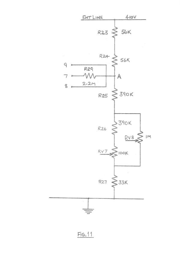
The latter quantity is R26 and RV7 in series plus
the parallel resistor RV8:-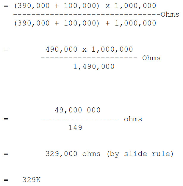
Thus, the total resistance, RT = (56K + 390K + 33K + 329K )
= 864K
Now, the amount of resistance between point A
(Fig, 11) and earth is:- = (390K + 329K + 33K) = 752K
Thus, since the EHT line is at 41OV., the voltage
(in theory) at point A is:-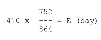
E = 357 Volts and this is the theoretical
voltage on the C.R.T. pins 7., 8 and 9.
Now, if we measure this voltage by connecting
the voltmeter between point ‘A’ and earth , we in-
introduce an error because to register at all,the
meter must draw some current from the circuit.
This extra current will, therefore, also flow through
R23 and R24 and lower the voltage at point A the
actual amount depending on the resistance of the
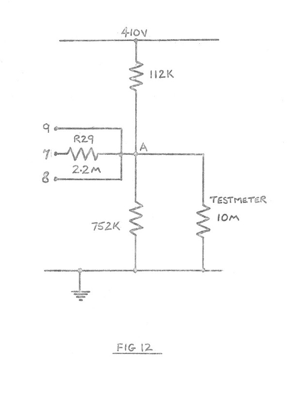
test-meter. Suppose that we use a test-meter of
total internal resistance of 10 Mohms. The set-
up, when the meter is connected in circuit as shown
in Fig. 12 and here the resistors between the
EHT line and point A in Fig.11 have been totalled
as have the resistors between point A and earth in
Fig. 11.
Thus, the new value for the total resistance between point
A and earth is that found by using the formula for resistors in
parallel, using the 752K and the 10M as values. This is:-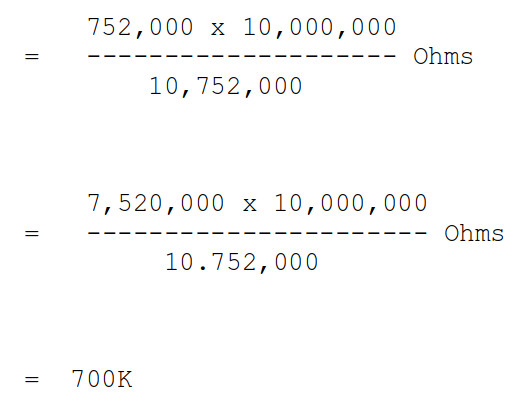
Therefore, the new value for the voltage between point
A and earth (and this will be indicated on the meter face) is:-
Thus,we have already "lost" (357 - 354) 3 volts by
connecting the meter positive terminal to point A. Suppose
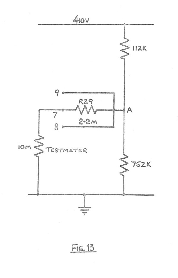
now that we connect the same test-meter to pin 7 of the
C.R.T and earth. This set-up is shown in Fig. 13 and you
can see that the extra current drawn by the meter will also
flow through R29.
The total resistance of Fig. 13 is the test-meter in series
with R29., both in parallel with the 752K and the whole in
series with the 112K. This 1s:-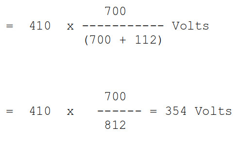
Thus,we have already "lost" (357 - 354) 3 volts by
connecting the meter positive terminal to point A. Suppose
now that we connect the same test-meter to pin 7 of the
C.R.T and earth. This set-up is shown in Fig. 13 and you
can see that the extra current drawn by the meter will also
flow through R29.
The total resistance of Fig. 13 is the test-meter in series
with R29., both in parallel with the 752K and the whole in
series with the 112K. This is:-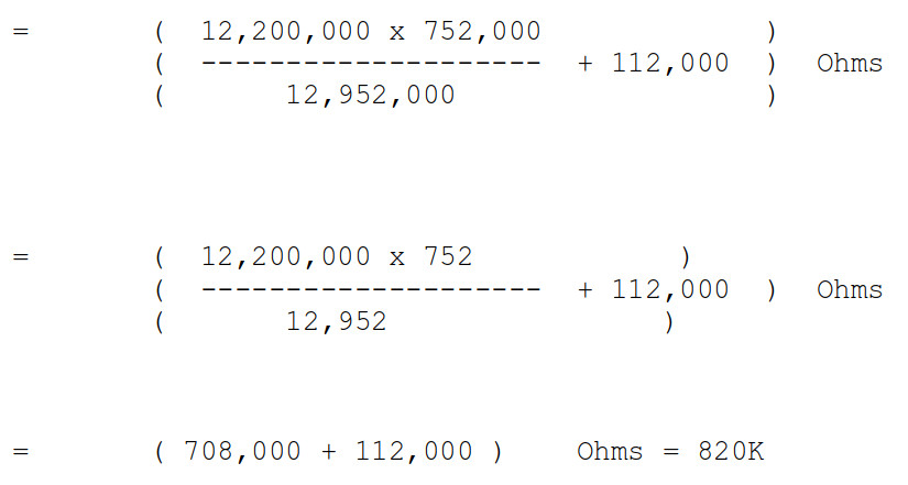
Therefore, the total current is, by 0hm's Law,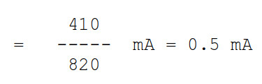
Because all this current flows through the 112K the new
voltage at point A is = (410 - 0.5 x 112) Volts
= (410 - 56) Volts
= 354 Volts.
The current through the 752K resistor in Fig. 13 is thus:
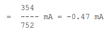
so that (0.5 - 0.47) mA must flow through R29 and the test-meter.
The voltage indicated on the test-meter is thus that at
point A in Fig. 13 less the "volts drop" across R29 and this
is:-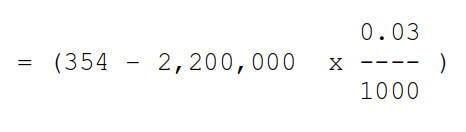
= (354 - 2,200 x 0.03) Volts
= 288 Volts :::::::::::::::::
Thus, although measurements suggest that C.R.T. pin 7 is
some 66 volts below that on Pins 8 & 9., theory tells us that
Pins 7., 8 and 9 are all at the same voltage and the error is
caused by the test-meter.
We hope that this diversion will vividly illustrate how
careful you must be when making measurements in electronics.
Do not forget that the "total resistance" of the Oscilloscope
Y-input is only about 1M-Ohm i.e. one tenth or the test meter's
total resistance !
We shall now return to our examination of the Oscilloscope,
continuing with Y-Amplifier and its attenuator.
The Y-Amplifier_and Attenuator
The components forming this part of the Oscilloscope are
shown in Diagram 5. The function of each component is as follows:
(a) RV1 - This is the Y-input attenuator. Because one
end of the potentiometer track is connected to earth, we can
"pick of" any voltage between that applied to the Y-input
socket and zero.
(b) C1 - If we use the Oscilloscope Y-test lead to look
at the anode of a valve, for example; in addition to picking
off the alternating voltage, we shall get the relatively high
Voltage, (which is a direct voltage, i.e. fixed) also present.
If this steady voltage were to be applied to the control grid
(2) or V1., it would upset the operation of the Y-amplifier
so it is necessary to 'block' the DC component or an applied
Signal. This ‘blocking’ function is carried out by C1. In-
cidentally, it is the maximum permitted voltage (DC) on C1
that limits the maximum input to the Oscilloscope. This value,
Written on the body of the capacitor, is 350V.
(c) R4 - This resistor forms the anode load for V1., (As
it is not the intention here to discuss valve operation in
detail, only the "names" of components will be quoted so that
You can identify them when studying valves from a text-book).
(d) C2 - This capacitor stops the fixed, steady voltage
on the Y2-plate from upsetting the action or V1. The amplified
signal, will, of course, pass "through" C2 because it is an
alternating voltage.
(e) R6 and R7 - These resistors supply the screen grid (8)
voltage for V1. They are connected up to form a potential
divider network across the HT line and earth.
(f) C4 - This capacitor helps to stabilise the screen grid
(8) voltage which would otherwise alternate slightly in opposition
to the signal voltage. This would reduce the amplification of
the stage.
(g) R5 and C3 - R5 provides for cathode bias in the V1
circuit and C3 acts (much as C4 does) to stabilise the voltage on the cathode and avoid loss of amplification.
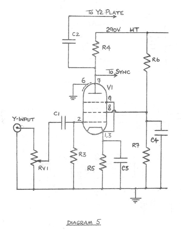
(h) R3 - This is the grid resistance of V1. Without it,
the charge which accumulates on the control grid (2)
would not be able to drain away to earth. R3 also
provides a convenient path to earth for any leakage
current flowing through C1.
This complete examination of the Y-amplifier and
thus just leaves the Timebase Circuit for investigation.
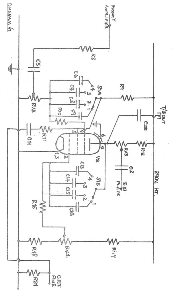
The Timebase Generator and Flyback Suppression Line.
The relevant components for this part of the circuit
are shown in Diagram 6. To explain in detail how the
circuit operates would be long and difficult, but students
who are interested should study the transitron oscillator.
This functions basically by applying a higher potential.
to the screen grid than is applied to the anode. This
unusual arrangement, coupled with a property of the valve
known as the Miller Effect, causes the Timebase valve, V2,
to oscillate and produce a sawtooth voltage like that in
Figs.8(b) and 9(b).
The components that determine the frequency of the
oscillation are C13, C14, C15 and C16 (coarse control)
and R15, R17, R18 and RV4 (this control provides fine-
frequency adjustment).
In order that we can maintain a stable picture on
the C.R.T., a small portion of the Y-amplifier output is
fed into the Timebase Generator valve and this can slightly
adjust the Timebase Frequency (in sympathy with applied
signal frequency) to keep the display steady, the
components that perform this function are R8, C5, RV2
(fine sync control) C6, C7, C8, C9 (coarse Sync control)
R9 and R10.
The small negative pulses needed for flyback suppression
appear on the screen grid (8) of V2 and are coupled to the
C.R.T. through R11 and C11.
The function of the remaining components is:-
(a) R12 and RV3 - These provide the anode load for V2.
Additionally, RV3 operates as a width control by
varying the amount of the T/Base voltage swing fed
to the C.R.T. X1-plate via C18.
(b) C18 - This capacitor blocks the fixed voltage on
the X1-plate and stops it from upsetting V2's operation.
(c) C22 - The voltage which exists on V2 anode (7) is a
composite of a fixed voltage plus an alternating part.
To stop the fixed voltage from getting out of the
TIMEBASE OUTPUT SOCKET,capacitor C22 is fitted.
Therefore, only the alternating part of the V2-anode (7)
voltage appears at T/B.OUT.
(d) R21 - This resistor couples the cathode bias to the
control grid (2) of the C.R.T. thus ensuring that
the correct potential difference between cathode (3)
and control grid (2) always exists.
That concludes our examination of the "Lernakit"
Oscilloscope. It is our hope that you will now have a
better understanding of the instrument and that any points
not clear to you will stimulate your interest and cause
you to read further into the theory of valve circuits.